Adresse de livraison

Bonjour! Se connecter ou Inscrivez-vous immédiatement
APP Fiche technique Direct 290K likes Utsource

Puces CI
Circuits intégrés numériques de la série 74
Circuits intégrés numériques de la série CD40
Coupleurs optiques
CIs horloge et calculatrice
Amplificateurs opérationnels
CIs interrupteurs de puissance
CIs pilote
Mémoire flash
Mémoire
Audio à usage spécifique
Horloge/Temporisation - Applications spécifiques
Horloge/Temporisation - Tampons d'horloge, conducteurs
Horloge/Temporisation - Générateurs d'horloge, BVP, Synthétiseurs de fréquence
Horloge/Temporisation - Lignes de retard
Horloge/Temporisation - Batteries CI
Horloge/Temporisation - Minuteries et oscillateurs programmables
Horloge/Temporisation - Horloges en temps réel
Acquisition de données - ADCs/CADs - Objectif spécifique
Acquisition de données - Frontal analogique (AFE)
Acquisition de données - Convertisseurs analogique-numérique (ADC)
Acquisition de données - Potentiomètres numériques
Acquisition de données - Convertisseurs numérique-analogique (DAC)
Acquisition de données - Contrôleurs à écran tactile
Embarqué - CPLD (Complex Programmable Logic Devices)
Embarqué - DSP (Digital Signal Processors)
Embarqué - FPGA (Field Programmable Gate Array)
Embarqué - FPGA (Field Programmable Gate Array) avec Microcontrôleurs
Embarqué - Modules microcontrôleur, microprocesseur, FPGA
Embarqué - Microcontrôleurs
Embarqué - Microcontrôleurs - Applications spécifiques
Embarqués - Microprocesseurs
Embarqué - PLD (Programmable Logic Device)
Embarqué - Système sur puce (SoC)
Interface - Interrupteurs analogiques - usage spécifique
Interface - Commutateurs analogiques, multiplexeurs, démultiplexeurs
Interface - CODECs
Interface - Contrôleurs
Interface - Synthèse numérique directe (DDS)
Interface - Pilotes, Récepteurs, Émetteurs-récepteurs
Interface - Encodeurs, décodeurs, convertisseurs
Interface - Filtres - Actifs
Interface - Expandeurs d'E/S
Interface - Modems - Circuits intégrés et modules
Interface - Modules
Interface - Interfaces de capteurs et de détecteurs
Interface - Capteur, Tactile capacitif
Interface - Sérialiseurs, désérialiseurs
Interface - Tampons, Répéteurs, Séparateurs de signaux
Interface - Terminateurs de signaux
Interface - Spécialisée
Interface - Télécommunications
Interface - UARTs (Universal Asynchronous Receiver Transmitter)
Interface - Enregistrement et lecture de la voix
Linéaire - Amplificateurs - Audio
Linéaire - Amplificateurs - Instrumentation, Ampoules OP, Ampoules tampons
Linéaire - Amplificateurs - usage spécial
Linéaire - Amplificateurs - Amplificateurs et modules vidéo
Linéaire - Multiplicateurs analogiques, diviseurs
Linéaire - Comparateurs
Linéaire - Traitement vidéo
Logique - Tampons, pilotes, récepteurs, émetteurs-récepteurs
Logique - Comparateurs
Logique - Compteurs, diviseurs
Logique - Mémoire FIFO
Logique - Flip Flops
Logique - Portes et onduleurs
Logique - Portes et onduleurs - multifonctionnels, configurables
Logique - Loquets
Logique - Multivibrateurs
Logique - Générateurs de parité et contrôleurs
Logique - Registres des équipes
Logique - Commutateurs de signaux, multiplexeurs, décodeurs
Logique - Logique de spécialité
Logique - Traducteurs, changeurs de niveau
Logique - Fonctions universelles des bus
Mémoire - Batteries
Mémoire - Proms de configuration pour les FPGA
Mémoire - Contrôleurs
PMIC - Convertisseurs CA-CC, commutateurs hors ligne
PMIC - Chargeurs de batterie
PMIC - Gestion des batteries
PMIC - Réglementation/gestion actuelle
PMIC - Pilotes d'affichage
PMIC - Compteurs d'énergie
PMIC - Chauffeurs à pont complet et à demi-pont
PMIC - Conducteurs de porte
PMIC - Contrôleurs d'échange à chaud
PMIC - Pilotes de laser
PMIC - Pilotes LED
PMIC - Éclairage, contrôleurs de ballast
PMIC - Conducteurs de véhicules, contrôleurs
PMIC - Contrôleurs OR, Diodes Idéales
PMIC - PFC (Correction du facteur de puissance)
PMIC - Interrupteurs de distribution de courant, conducteurs de charge
PMIC - Gestion de l'énergie - Spécialisé
PMIC - Contrôleurs d'alimentation par Ethernet (PoE)
PMIC - Contrôleurs d'alimentation électrique, moniteurs
PMIC - Convertisseurs RMS vers DC
PMIC - Contrôleurs
PMIC - Gestion thermique
PMIC - Convertisseurs V/F et F/V
PMIC - Référence de tension
PMIC - Régulateurs de tension - Contrôleurs de commutation DC
PMIC - Régulateurs de tension - Régulateurs à découpage DC
PMIC - Régulateurs de tension - Linéaire
PMIC - Régulateurs de tension - Linéaire + commutation
PMIC - Régulateurs de tension - Régulateurs linéaires
PMIC - Régulateurs de tension - Usage spécial
CIs spécialisés
Modules
IGBT
IPM
Thyristors
Rectificateurs
Alimentation électrique
Module d'alimentation intelligent
SCR, GTO et Diode
FET
Transistors Darlington
Modules RF
PRODUITS CNC
ENCODEUR
Moteur
Servomoteur & amplificateur & servo
Module de diodes
Module à transistors
Relais de commutation
PLC
Onduleur
Contacteur et briseur
Conseil des ascenseurs
Contrôle de l'industrie
Transistors
Diode
Transistors bipolaires
Résistances
Résistances à Couche de Carbone
Résistances de Ciment
Résistances à Montage sur Châssis
Circuit de Résistance - Surface de Montage
Résistances de Détection de Courant
Résistance du Circuit Fusible
Résistances Haute Précision CMS et Faible TCR
Résistance Haute Tension
Résistances de Bande LED
Résistance MELF
Résistances en Alliage Métallique
Résistance en Film Métallique (TH)
Résistances de Glaçure Métalliques
Résistances à Couche d'Oxyde Métallique
Résistances à Oxyde Métallique
Thermistance CTN
Thermistance PTC
Photorésistances
Potentiomètres et Résistances Variables
Potentiomètre de Précision
Réseaux de Résistances et Tableaux
Réseaux et Groupements de Résistances (TH)
Résistances Ultra Basses (SMD)
Résistances Variables
Varistance
Résistances Bobinées
Condensateurs
Condensateurs Électrolytiques en Aluminium - CMS
Condensateur CL21
Condensateurs à Disque en Céramique
Condensateurs Haute Tension
Condensateur à Film Polyester Métallisé
Condensateurs à Multicouches Céramique MLCC - Plombé
Condensateurs à Multicouches Céramique MLCC - SMD / SMT
Condensateur Mylar
Condensateurs à l'Oxyde de Niobium
Condensateurs à Film de Polyester
Condensateur Électrolytique à Polymère Solide
Supercondensateurs et Ultracondensateurs
Condensateurs de Suppression
Condensateurs au Tantale
Condensateur, Condensateurs Variables
Inducteurs et Perles de Ferrite et Transformateurs
Antennes
Transformateurs de Courant
Inducteurs Généraux (TH)
Inducteurs HF
Inducteurs (SMD)
Filtre de Ligne
Inducteurs de Puissance
Transformateur Électrique
Transformateur RJ45
Inducteur Radial (TH)
Les Inducteurs Circulaires
Cristaux
49S
49SMD
49U
Résonateurs en Céramique
Oscillateurs DIP (XO)
Cristaux de Cylindre Radiaux
Résonateurs SAW
Cristaux SMD
Oscillateurs SMD (XO)
Connecteurs
Connecteurs AV
Connecteurs Audio et Vidéo
Banane et Connecteurs de Pointe
Connecteurs de Bord de Carte
Connecteurs Circulaires
Connecteur - Prises de Carte
Connecteurs
Connecteurs - Accessoires
Connecteurs - Boîtiers
Contacts
Connecteurs D-sub
Connecteurs Ethernet / Connecteurs Modulaires
Connecteurs FFC, FPC (Flexibles Plats)
Connecteurs de Fibre Optique
Supports IC et Composants
Conduits de Lumière Led
Connecteurs Mezzanine (Carte à Carte)
Connecteurs PCB - Embases, Broches Mâles
Connecteurs PCB - Embases, Réceptacles, Prises Femelles
Connecteurs PCB - Boîtiers
Connecteurs d'Alimentation
Connecteurs RF / Connecteurs Coaxiaux
Shunts & Jumpers
Borniers - Accessoires
Borniers - Blocs Barrières
Borniers - Rail Din, Canal
Borniers - En-têtes, Fiches et Prises
Bornes
Attaches
Points de Test / Anneaux de Test
Prises USB
Connecteurs non Spécifiés
Câblage à Vis
Câblage à Ressort
Borniers Enfichables
Borniers Traversants
Terminaux automobiles
Boîtiers de bornes, manchons et blocs isolants
Connecteurs et bornes de fil à déconnexion rapide
Outillage de rechange et d'usure
Connecteurs automobiles
Connecteurs PCB
SFP émetteurs-récepteurs optiques
100BASE SFP
1000BASE SFP
CWDM SFP
DWDM SFP
BIDI SFP
SONET/SDH SFP
2G/4G FC SFP
Customized SFP
SFP+ émetteurs-récepteurs optiques
10G SFP+
BiDi SFP+
CWDM SFP+
DWDM SFP+
8G/16G FC SFP+
Customized SFP+
XFP émetteurs-récepteurs optiques
10G XFP
BIDI XFP
CWDM XFP
DWDM XFP
Customized XFP
40G/100G émetteurs-récepteurs optiques
40G QSFP+
100G QSFP28
100G CFP
100G CFP2
100G CFP4
Customized 40G/100G
25G SFP28
100G CXP
40G BiDi QSFP+
Câbles optiques actifs
10G SFP+ to SFP+ AOC
40G QSFP+ to QSFP+ AOC
40G QSFP+ to 4xSFP+ AOC
40G QSFP+ to 8xLC AOC
100G QSFP28 AOC
Customized AOC
25G SFP28 AOC
100G QSFP28 to 4xSFP28 AOC
56G QSFP+ to QSFP+
Câble de raccordement direct
10G SFP+ to SFP+ DAC
40G QSFP+ to QSFP+ DAC
40G QSFP+ to 4xSFP+ DAC
25G SFP28 to SFP28 DAC
100G QSFP28 to QSFP28 DAC
100G QSFP28 to 4 SFP28 DAC
Customized DAC
56G QSFP+ to QSFP+
Câble HDMI du fibre optique
Optical Fiber Patch Cable
MTP/MPO Plenum Trunks
MTP/MPO-LC Plenum
MTP/MPO LSZH Trunks
MTP/MPO-LC LSZH
OM4 40 100Gb 50/125 Multimode
OM3 10Gb 50/125 Multimode
OM2 50/125 Multimode
OM1 62.5/125 Multimode
OS2 9/125 Singlemode Simplex
OS2 9/125 Singlemode Duplex
OM5 40G 100G 50/125 Multimode
Switchable LC Cables
Uniboot LC Cables
Ultra Low Loss LC SMF
Ultra Low Loss LC MMF
BIF Fiber Cables
Armored Patch Cables
Autres émetteurs-récepteurs
Converter Modules
3G/HD-SDI SFP
GBIC Transceivers
PON Transcievers
Transceiver Accessories
Capteurs de Température
Interrupteur de Commande de Température
Capteur de température et d'humidité
Capteur de poussière
Capteur PM 2.5
Capteur de gaz
Capteur de gaz combustible
Capteur d'alcool
Capteur de CO
Capteur d'hydrogène
Capteur de H2S
Capteur de CO2
Ammonia Sensor
Capteur de formaldéhyde
Capteur PIR
Autres capteurs
Capteur de fréquence cardiaque
Capteur optique
Capteur de couleur
Capteur à ultrasons
Capteur de champ magnétique
Capteur de courant électrique
Capteur de tension
Capteur de niveau liquide
Capteur de pression atmosphérique
Capteur météo
Capteur d'angle d'inclinaison
Capteur de mouvement
Capteur tactile
Capteur de flamme
Capteur de vibration
Capteur de vitesse
Modules LED
LED de forte puissance
LED SMD
LED rétroéclairage LED
LED COB
Afficheur LED
LED enfichable
Induction infrarouge
Piranha LED
Ampoule LED
Tube LED
Puce LED
Plaquette épitaxiale LED
LED de lumière rouge
LED de lumière orange
LED de lumière jaune
LED de lumière jaune-verte
LED de lumière verte
LED de lumière bleue
LED de lumière violette
LED de lumière blanche
Autres puces LED
Afficheurs LED

Se connecter
-
0
-
acheter(0)
-
Demandes d'offres (0)

-


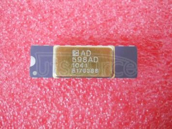
 Required
 signal conditioning subsystem. It is used in conjunction with LVDTs to convert transducer mechanical position to a unipolar or bipolar dc voltage with a high degree of accuracy and repeatability. All circuit functions are included on the chip. With the addition of a few external passive components to set frequency and gain, the AD598 converts the raw LVDT secondary output to a scaled dc signal. The device can also be used with RVDT transducers.
The AD598 contains a low distortion sine wave oscillator to drive the LVDT primary. The LVDT secondary output consists of two sine waves that drive the AD598 directly. The AD598 operates upon the two signals, dividing their difference by their sum, producing a scaled unipolar or bipolar dc output.
The AD598 uses a unique ratiometric architecture (patent pending) to eliminate several of the disadvantages associated with traditional approaches to LVDT interfacing. The benefits of this new circuit are: no adjustments are necessary, transformer null voltage and primary to secondary phase shift does not affect system accuracy, temperature stability is improved, and transducer interchangeability is improved.")