Indirizzo di spedizione

Ciao! Accesso O Registra immediatamente
APP Libretto dei dati Trasmissione in diretta 290K likes Utsource

Chip circuito integrato
Circuiti integrati digitali serie 74
Circuiti integrati digitali serie CD40
Accoppiatori ottici
Orologio e calcolatrice di circuiti integrati
Amplificatori operazionali
Interruttore di accensione circuito integrato
Driver circuito integrato
Memoria flash
Memoria
Audio speciale
Clock/ Timing - Specifico per l'applicazione
Clock/ Timing - Drivers, buffer orologio
Clock/ Timing - Generatori orologio, PLL, sintetizzatori di frequenza
Clock/ Timing - Linee di ritardo
Clock/ Timing - Batterie circuito integrato
Clock/ Timing - Oscillatori e Timer programmabili
Clock/ Timing - Clock in Real Time
Acquisizione dati - ADC / DAC - Scopo speciale
Acquisizione dati - Front end analogico (AFE)
Acquisizione dati - Convertitore da analogico a digitale (ADC)
Acquisizione dati - Potenziometro digitale
Acquisizione dati - Convertitore da digitale ad analogico (ADC)
Acquisizione dati - Controller Touch-screen
Incorporato - CPLD (dispositivi logici programmabili complessi)
Incorporato - DSP ( processori segnali digitali)
Incorporato - FPGA ( dispositivi programmabili)
Incorporato - FPGA ( dispositivi programmabili) con microcontroller
Incorporato - Microcontroller, Microprocessori, Moduli FPGA
Incorporato - Microcontroller
Incorporato - Microcontroller - Specifica Applicazione
Incorporato - Microprocessori
Incorporato - PLD (dispositivo logico programmabile)
Incorporato - Sistema su chip (SoC)
Interfaccia - Interruttori analogici - Scopo speciale
Interfaccia - Interruttori analogici, multiplexer, demultiplexer
Interfaccia - CODEC
Interfaccia - Controller
Interfaccia - Sintesi digitale diretta (DSS)
Interfaccia - Driver, Ricevitori, Transceiver
Interfaccia - Codificatori, Decodificatori, Convertitori
Interfaccia - Filtri - Attivi
Interfaccia - Espansori I / O
Interfaccia - Modem - CI e moduli
Interfaccia - Moduli
Interfaccia - Interfacce sensore e rilevatore
Interfaccia - Sensore, Touch Capacitivo
Interfaccia - Serializzatori, Deserializzatori
Interfaccia - Buffer di segnale, Ripetitori, Splitter
Interfaccia - Terminatori di segnale
Interfaccia - Specializzato
Interfaccia - Telecom
Interfaccia - UART (Trasmettitore Asincrono Universale del Ricevitore)
Interfaccia - Registrazione e Riproduzione vocale
Lineare - Amplificatori - Audio
Lineari - Amplificatori - Strumentazione, Amplificatori operazionali, Amplificatori buffer
Linear - Amplificatore - Scopo speciale
Lineare - Amplificatore - Amplificatore Video e Moduli
Lineari - Moltiplicatori analogici, Divisori
Lineare - Comparatori
Lineare - Elaborazione video
Logica - Buffer, Driver, Ricevitori, Transceiver
Logica - Comparatori
Logica - Contatori, Divisori
Logica - Memoria FIFO
Logica - Flip Flops
Logica - Gate e Inverter
Logica - Gate e Inverter - Multifunzione, Configurabile
Logica - Latch
Logica - Multivibratori
Logica - Generatori e Controllori di parità
Logica - Registri a scorrimento
Logica - Interruttori di segnale, Multiplexer, Decodificatori
Logica - Logica speciale
Logica - Traduttori, Cambi di livello
Logica - Funzioni Bus Universale
Memoria - Batterie
Memoria - Proms di configurazione per FPGA
Memoria - Controller
PMIC - Convertitori ca-cc, Commutatori offline
PMIC - Caricabatterie
PMIC - Gestione della batteria
PMIC - Regolamentazione / Gestione attuale
PMIC - Driver di visualizzazione
PMIC - Misurazione dell'energia
PMIC - Driver full-half-bridge
PMIC - Drivers Gate
PMIC - Controller Hot Swap
PMIC - Driver laser
PMIC - Driver LED
PMIC - Illuminazione, Regolatori di zavorra
PMIC - Driver per motori, Controller
PMIC - Controller OR, Diodi ideali
PMIC - PFC (correzione del fattore di potenza)
PMIC - Interruttori di distribuzione dell'alimentazione, Driver di caricamento
PMIC - Power Management - Specializzato
PMIC - Controller Power Over Ethernet (PoE)
PMIC - Controller di alimentazione, Monitor
PMIC - Convertitori da RMS a CC
PMIC - Supervisori
PMIC - Gestione termica
PMIC - Convertitori V / F e F / V
PMIC - Riferimento di tensione
PMIC - Regolatori di tensione - Controllori a commutazione cc-cc
PMIC - Regolatori di tensione - Regolatori a commutazione cc-cc
PMIC - Regolatori di tensione - Lineari
PMIC - Regolatori di tensione - Lineari + commutazione
PMIC - Regolatori di tensione - Controllori regolatori lineari
PMIC - Regolatori di tensione - Scopo speciale
CI Specializzati
Moduli
IGBT
IPM
Tiristori
Raddrizzatori
Alimentazione elettrica
Modulo Smart Power
SCR, GTO e Diodo
FET
Transistor Darlington
Moduli RF
PRODOTTI CNC
CODIFICATORE
Motore
Servo Drive & Amplificatore & Servo
Modulo Diodo
Modulo Transistor
Relè di Commutazione
PLC
Invertitore
Contattore e Interruttore
Scheda Ascensore
Controllo Settore
Transistor
Diodo
Transistor bipolari
resistenze
Resistori a film di carbonio
Resistori di cemento
Resistori per montaggio su telaio
Resistore a chip - Montaggio superficiale
Resistori rilevatori di corrente
Resistore a chip fusibile
Resistori SMD ad alta precisione e bassa TCR
Resistori ad alta tensione
Resistori a strisce LED
Resistori MELF
Resistori in lega metallica
Resistori a film metallico (TH)
Resistori di smalto metallico
Resistori a film di ossido di metallo
Resistori all'ossido di metallo
Termistori NTC
Termistori PTC
Fotoresistenze
Potenziometri e resistori variabili
Potenziometro di precisione
Reti e array di resistori
Reti e array di resistori (TH)
Resistori Ultrabassi (SMD)
Resistori variabili
Varistori
Resistori ad avvolgimento
Condensatori
Condensatori elettrolitici in alluminio - SMD
Condensatore CL21
Condensatori a dischi ceramici
Condensatori ad alta tensione
Condensatore in film di poliestere metallizzato
Condensatori ceramici multistrato MLCC - Piombo
Condensatori ceramici multistrato MLCC - SMD&SMT
Condensatore di Mylar
Condensatori all'ossido di niobio
Condensatori a film di poliestere
Condensatore elettrolitico polimero solido
Supercondensatori e Ultracondensatori
Condensatori di soppressione
Condensatori al tantalio
Trimmer, condensatori variabili
Induttori e trasformatori di ferrite
Antenne
Trasformatori di correnti
Induttori Generali (TH)
Induttori HF
Induttori (SMD)
Filtro LINE
Induttori di potenza
Trasformatore di potenza
Trasformatore RJ45
Induttore radiale (TH)
Gli induttori circolari
Crystals
49S
49SMD
49U
Risonatori ceramici
Oscillatori DIP (XO)
Cristalli a cilindro radiale
Risuonatori SAW
Cristalli SMD
Oscillatori SMD (XO)
Connettori
Connettori AV
Connettori audio e video
Connettori a banana e punta
Connettori bordo scheda
Connettori circolari
Connettore - Prese per schede
Connettori
Connettori-Accessori
Connettori- Alloggiamenti
Contatti
Connettori D-Sub
Connettori Ethernet&Connettori modulari
Connettori FFC, FPC (flessibile piatto)
Connettori in fibra ottica
Prese per circuiti integrati e componenti
Tubi luminosi a LED
Connettori mezzanine (da scheda a scheda)
Connettori PCB - Basette, pin maschio
Connettori PCB - Basette, prese, prese femmina
Connettori PCB - Alloggiamenti
Connettori di alimentazione
Connettori RF&Connettori coassiali
Shunt e ponticelli
Morsettiere - Accessori
Morsettiere - Blocchi a barriera
Morsettiere - Din Rail, canale
Morsettiere - Basette, spine e prese
Terminali
Clip di prova
Punti di prova&anelli di prova
Connettori USB
Connettori non specificati
Cablaggio a vite
Cablaggio a molla
Morsettiere innestabili
Morsettiere passanti
Terminali automobilistici
Alloggiamenti terminali, guaine isolanti e blocchi
Connettori e terminali per cavi a scollegamento rapido
Utensili di ricambio e usura
Connettori automobilistici
Connettori PCB
Transcevitori SFP
100BASE SFP
1000BASE SFP
CWDM SFP
DWDM SFP
BIDI SFP
SONET/SDH SFP
2G/4G FC SFP
Customized SFP
SFP + Transcevitori
10G SFP+
BiDi SFP+
CWDM SFP+
DWDM SFP+
8G/16G FC SFP+
Customized SFP+
Transcevitori XFP
10G XFP
BIDI XFP
CWDM XFP
DWDM XFP
Customized XFP
Transcevitori 40G/100G
40G QSFP+
100G QSFP28
100G CFP
100G CFP2
100G CFP4
Customized 40G/100G
25G SFP28
100G CXP
40G BiDi QSFP+
Cavi Ottici Attivi
10G SFP+ to SFP+ AOC
40G QSFP+ to QSFP+ AOC
40G QSFP+ to 4xSFP+ AOC
40G QSFP+ to 8xLC AOC
100G QSFP28 AOC
Customized AOC
25G SFP28 AOC
100G QSFP28 to 4xSFP28 AOC
56G QSFP+ to QSFP+
Cavi A Presa Diretta
10G SFP+ to SFP+ DAC
40G QSFP+ to QSFP+ DAC
40G QSFP+ to 4xSFP+ DAC
25G SFP28 to SFP28 DAC
100G QSFP28 to QSFP28 DAC
100G QSFP28 to 4 SFP28 DAC
Customized DAC
56G QSFP+ to QSFP+
Cavo HDMI fibra ottica
Optical Fiber Patch Cable
MTP/MPO Plenum Trunks
MTP/MPO-LC Plenum
MTP/MPO LSZH Trunks
MTP/MPO-LC LSZH
OM4 40 100Gb 50/125 Multimode
OM3 10Gb 50/125 Multimode
OM2 50/125 Multimode
OM1 62.5/125 Multimode
OS2 9/125 Singlemode Simplex
OS2 9/125 Singlemode Duplex
OM5 40G 100G 50/125 Multimode
Switchable LC Cables
Uniboot LC Cables
Ultra Low Loss LC SMF
Ultra Low Loss LC MMF
BIF Fiber Cables
Armored Patch Cables
Altri transcevitori
Converter Modules
3G/HD-SDI SFP
GBIC Transceivers
PON Transcievers
Transceiver Accessories
Sensori di Temperatura
Temperatura passare
Sensore Temperatura e Umidità
Sensore Polvere
Sensore PM2.5
Sensore Gas
Sensore Gas Combustibile
Sensore di alcol
Sensore CO
Sensore Idrogeno
Sensore H2S
Sensore CO2
Ammonia Sensor
Sensore Formaldeide
Sensore PIR
Altri Sensori
Sensore Frequenza Cardiaca
Sensore Ottico
Sensore di Colore
Sensore Ultrasuoni
Sensore Campo Magnetico
Sensore Corrente Elettrica
Sensore Tensione
Sensore Livello Liquidi
Sensore Pressione Atmosferica
Sensore Meteorologico
Sensore Angolo Inclinazione
Sensore Gesti
Sensore Tattile
Sensore Fiamma
Sensore Vibrazione
Rilevatore Velocità
Moduli LED
LED Alta-Potenza
SMD LED
Luce posteriore LED
COB LED
Display LED
Presa LED
Induzione Infrarossi
LED Piranha
Lampadine LED
Diodo Illuminato
Chip A Illuminazione LED
Fette Epilessiali LED
LED Luce-Rossa
LED Luce-Arancione
LED Luce-Gialla
LED Luce Verde-Gialla
LED Luce-Verde
LED Luce-Blu
LED Luce-Viola
LED Luce-Bianca
Altri Chip A Illuminazione LED
Display LED

-
0
-
Acquista(0)
-
Richiesta di prezzo (0)

-


 Required
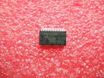
 signal conditioning subsystem. It is used in conjunction with LVDTs to convert transducer mechanical position to a unipolar or bipolar dc voltage with a high degree of accuracy and repeatability. All circuit functions are included on the chip. With the addition of a few external passive components to set frequency and gain, the AD598 converts the raw LVDT secondary output to a scaled dc signal. The device can also be used with RVDT transducers.
The AD598 contains a low distortion sine wave oscillator to drive the LVDT primary. The LVDT secondary output consists of two sine waves that drive the AD598 directly. The AD598 operates upon the two signals, dividing their difference by their sum, producing a scaled unipolar or bipolar dc output.
The AD598 uses a unique ratiometric architecture (patent pending) to eliminate several of the disadvantages associated with traditional approaches to LVDT interfacing. The benefits of this new circuit are: no adjustments are necessary, transformer null voltage and primary to secondary phase shift does not affect system accuracy, temperature stability is improved, and transducer interchangeability is improved.")