Nakliye adresi

Merhaba! Oturum aç veya Şimdi kaydolun
APP Veri sayfası Canlı Yayın 290K likes Utsource

IC Yongaları
74 serisi Dijital Tümleşik Devreler
CD40 serisi Dijital Tümleşik Devreler
Optik Kuplörler
Saat ve Hesap Makinesi IC'leri
İşlemsel Yükselteçler
Güç Anahtarı IC'leri
Sürücü Ic'leri
Flash Bellek
Hafıza
Ses Özel Amaçlı
Saat/Zamanlama - Uygulamaya Özel
Saat/Zamanlama - Saat Tampon Sürücüleri
Saat/Zamanlama - Saat Jeneratörleri PLL'ler Frekans Sentezleyicileri
Saat/Zamanlama - Gecikme Hatları
Saat/Zamanlama - IC Piller
Saat/Zamanlama - Programlanabilir Zamanlayıcılar ve Osilatörler
Saat/Zamanlama - Gerçek Zamanlı Saatler
Veri Toplama - ADC'ler/DAC'ler - Özel Amaçlı
Veri Toplama - Analog Ön Uç (AFE)
Veri Toplama - Analogdan Dijitale Dönüştürücüler (ADC)
Veri Toplama - Dijital Potansiyometreler
Veri Toplama - Dijitalden Analoğa Dönüştürücüler (DAC)
Veri Toplama - Dokunmatik Ekran Denetleyicileri
Gömülü - CPLD'ler (Karmaşık Programlanabilir Mantık Aygıtları)
Gömülü - DSP (Dijital Sinyal İşlemciler)
Gömülü - FPGA'lar (Alan Programlanabilir Kapı Dizisi)
Gömülü - Mikrodenetleyicili FPGA'lar (Alan Programlanabilir Kapı Dizisi)
Gömülü - Mikrodenetleyici Mikroişlemci FPGA Modülleri
Gömülü - Mikrodenetleyiciler
Gömülü - Mikrodenetleyiciler - Uygulamaya Özel
Gömülü - Mikroişlemciler
Gömülü - PLD'ler (Programlanabilir Mantık Aygıtı)
Gömülü - Yonga Üzerinde Sistem (SoC)
Arayüz - Analog Anahtarlar - Özel Amaçlı
Arayüz - Analog Anahtarlar Çoklayıcılar
Arayüz - CODEC'ler
Arayüz - Denetleyiciler
Arayüz - Doğrudan Dijital Sentez (DDS)
Arayüz - Sürücüler Alıcılar Telsizler
Arayüz - Kodlayıcılar Kod Çözücüler Dönüştürücüler
Arayüz - Filtreler - Aktif
Arayüz - G/Ç Genişleticiler
Arayüz - Modemler - IC'ler ve Modüller
Arayüz - Modüller
Arayüz - Sensör ve Dedektör Arayüzleri
Arayüz - Sensör Kapasitif Dokunmatik
Arayüz - Serileştiriciler Serileştiriciler
Arayüz - Sinyal Tamponları Tekrarlayıcılar Ayırıcılar
Arayüz - Sinyal Sonlandırıcılar
Arayüz - Özel
Arayüz - Telekom
Arayüz - UART'lar (Evrensel Asenkron Alıcı Verici)
Arayüz - Ses Kaydı ve Oynatma
Doğrusal - Amplifikatörler - Ses
Doğrusal - Yükselteçler - Enstrümantasyon OP Amperleri Tampon Amperleri
Doğrusal - Yükselteçler - Özel Amaçlı
Doğrusal - Amplifikatörler - Video Amplifikatörleri ve Modülleri
Doğrusal - Analog Çarpanlar Bölücüler
Doğrusal - Karşılaştırıcılar
Doğrusal - Video İşleme
Mantık - Tamponlar Sürücüler Alıcılar Telsizler
Mantık - Karşılaştırıcılar
Mantık - Sayaç Bölücüler
Mantık - FIFO Hafızası
Mantık - Flip Floplar
Mantık - Kapılar ve Eviriciler
Mantık - Kapılar ve Çeviriciler - Çok İşlevli Yapılandırılabilir
Mantık - Mandallar
Mantık - Multivibratörler
Mantık - Eşlik Üreteçleri ve Denetleyiciler
Mantık - Kaydırma Yazmaçları
Mantık - Sinyal Anahtarları Çoklayıcılar Kod Çözücüler
Mantık - Özel Mantık
Mantık - Çevirmenler Seviye Değiştiriciler
Mantık - Evrensel Veri Yolu İşlevleri
Bellek - Piller
Bellek - FPGA'lar için Yapılandırma Yönergeleri
Bellek - Denetleyiciler
PMIC - AC DC Dönüştürücüler Çevrimdışı Değiştiriciler
PMIC - Akü Şarj Cihazları
PMIC - Pil Yönetimi
PMIC - Mevcut Düzenleme/Yönetim
PMIC - Ekran Sürücüleri
PMIC - Enerji Ölçümü
PMIC - Tam Yarım Köprü Sürücüleri
PMIC - Kapı Sürücüleri
PMIC - Çalışırken Değiştirilebilir Denetleyiciler
PMIC - Lazer Sürücüleri
PMIC - LED Sürücüler
PMIC - Aydınlatma Balast Kontrolörleri
PMIC - Motor Sürücü Kontrol Cihazları
PMIC - OR Denetleyicileri İdeal Diyotlar
PMIC - PFC (Güç Faktörü Düzeltmesi)
PMIC - Güç Dağıtım Anahtarları Sürücüleri Yükler
PMIC - Güç Yönetimi - Uzmanlaşmış
PMIC - Ethernet Üzerinden Güç (PoE) Denetleyicileri
PMIC - Güç Kaynağı Denetleyicileri Monitörler
PMIC - RMS'den DC'ye Dönüştürücüler
PMIC - Süpervizörler
PMIC - Termal Yönetim
PMIC - V/F ve F/V Dönüştürücüler
PMIC - Voltaj Referansı
PMIC - Voltaj Regülatörleri - DC DC Anahtarlama Kontrolörleri
PMIC - Voltaj Regülatörleri - DC DC Anahtarlama Regülatörleri
PMIC - Voltaj Regülatörleri - Lineer
PMIC - Voltaj Regülatörleri - Lineer + Anahtarlama
PMIC - Voltaj Regülatörleri - Lineer Regülatör Kontrol Cihazları
PMIC - Voltaj Regülatörleri - Özel Amaçlı
Özel IC'ler
Modüller
IGBT
IPM
tristörler
Doğrultucular
Güç kaynağı
Akıllı Güç Modülü
SCRGTO ve Diyot
FET
Darlington Transistörler
RF Modülleri
CNC ÜRÜNLERİ
KODLAYICI
Motor
Servo sürücü ve amplifikatör ve Servo
Diyot Modülü
Transistör Modülü
Anahtar Rölesi
PLC
Çevirici
Kontaktör & Kesici
Asansör Panosu
Endüstri Kontrolü
transistörler
Diyot
bipolar transistörler
Dirençler
Karbon Film Dirençleri
Çimento Dirençleri
Şasi Montaj Dirençleri
Yonga Direnci - Yüzey Montajı
Akım Algılama Dirençleri
Eriyebilir Talaş Direnci
Yüksek Hassasiyet ve Düşük TCR SMD Dirençleri
Yüksek Gerilim Direnci
LED Şerit Dirençler
MELF Direnci
Metal Alaşımlı Dirençler
Metal Film Direnci (TH)
Metal Sır Dirençleri
Metal Oksit Film Dirençler
Metal Oksit Dirençler
NTC Termistörleri
PTC Termistörleri
fotodirençler
Potansiyometreler ve Değişken Dirençler
Hassas Potansiyometre
Direnç Ağları ve Dizileri
Direnç Ağları ve Dizileri (TH)
Ultra Düşük Dirençler (SMD)
Değişken Dirençler
varistörler
Tel sargılı dirençler
kapasitörler
Alüminyum Elektrolitik Kapasitörler - SMD
CL21 Kondansatör
Seramik Disk Kapasitörler
Yüksek Gerilim Kondansatörleri
Metalize Polyester Film Kapasitör
Çok Katmanlı Seramik Kondansatörler MLCC - Kurşunlu
Çok Katmanlı Seramik Kondansatörler MLCC - SMD/SMT
Mylar Kapasitör
Niyobyum Oksit Kondansatörler
Polyester Film Kapasitörler
Katı Polimer Elektrolitik Kondansatör
Süper kapasitörler ve Ultra kapasitörler
Bastırma Kondansatörleri
tantal kapasitörler
Düzelticiler Değişken Kapasitörler
İndüktörler ve Ferrit Boncuklar ve Transformatörler
Antenler
Akım transformatörleri
Genel İndüktörler (TH)
HF İndüktörleri
İndüktörler (SMD)
Hat filtresi
Güç İndüktörleri
Güç transformatörü
RJ45 Trafo
Radyal İndüktör (TH)
Dairesel indüktörler
kristaller
49S
49SMD
49U
Seramik Rezonatörler
DIP Osilatörleri(XO)
Radyal Silindir Kristalleri
TESTERE Rezonatörleri
SMD Kristalleri
SMD Osilatörleri(XO)
Konnektörler
AV Konnektörleri
Ses ve Video Konnektörleri
Muz ve Uç Konnektörleri
Kart Kenar Konnektörleri
Dairesel Konnektörler
Konnektör - Kart Yuvaları
Konnektörler
Konnektörler - Aksesuarlar
Konnektörler - Muhafazalar
Kişiler
D-Sub Konnektörler
Ethernet Konnektörleri/Modüler Konnektörler
FFC FPC (Düz Esnek) Konnektörler
Fiber Optik Konnektörler
IC ve Bileşen Soketleri
LED Işık Boruları
Ara Konnektörler (Karttan Karta)
PCB Konnektörleri - Başlıklar Erkek Pimler
PCB Konnektörleri - Başlıklar Prizler Dişi Soketler
PCB Konnektörleri - Muhafazalar
Güç Konnektörleri
RF Konnektörleri/Koaksiyel Konnektörler
Şantlar ve Süveterler
Klemensler - Aksesuarlar
Klemensler - Bariyer Blokları
Klemensler - Din Ray Kanalı
Klemensler - Başlıklar Fişler ve Soketler
Terminaller
Test Klipleri
Test Noktaları/Test Halkaları
USB Konnektörleri
Belirtilmemiş Bağlayıcılar
Vidalı kablolama
Yay tipi kablolama
Tak-Çıkar Terminal Blokları
Duvar Klemensleri
Otomotiv Terminalleri
Terminal Muhafazaları Yalıtım Manşonları ve Blokları
Hızlı Ayırma Tel Konnektörleri ve Terminaller
Yedek ve Aşınma Aletleri
Otomotiv Konnektörleri
PCB Konnektörleri
SFP alıcı-vericileri
100BASE SFP
1000BASE SFP
CWDM SFP'si
DWDM SFP'si
BIDI SFP'si
SONET/SDH SFP'si
2G/4G SFP
Özelleştirilmiş SFP
SFP+ Alıcı-vericiler
10G SFP+
BiDi SFP+
CWDM SFP+
DWDM SFP+
8G/16G SFP+
Özelleştirilmiş SFP+
XFP Alıcı-Vericileri
10G XFP
BIDI XFP'si
CWDM XFP'si
DWDM XFP'si
Özelleştirilmiş XFP
40G/100G Alıcı-Vericiler
40G QSFP+
100G QSFP28
100G CFP
100G CFP2
100G CFP4
25G SFP28
100G Müşteri Deneyimi
Özelleştirilmiş 40G/100G
40G BiDi QSFP+
Aktif Optik Kablolar
10G SFP+'dan SFP+ AOC'ye
40G QSFP+'dan QSFP+ AOC'ye
40G QSFP+ - 4xSFP+ AOC
40G QSFP+'dan 8xLC AOC'ye
100G QSFP28 AOC
Özelleştirilmiş AOC
25G SFP28 AOC
100G QSFP28 - 4xSFP28 AOC
56G QSFP+'dan QSFP+'ya
Doğrudan Bağlantı Kabloları
10G SFP+'dan SFP+ DAC'a
40G QSFP+'dan QSFP+ DAC'ye
40G QSFP+ - 4xSFP+ DAC
25G SFP28'den SFP28 DAC'ye
100G QSFP28'den QSFP28 DAC'ye
100G QSFP28 - 4 SFP28 DAC
Özelleştirilmiş DAC
56G QSFP+'dan QSFP+'ya
Fiber optik HDMI kablosu
Fiber Optik Yama Kablosu
MTP/MPO Plenum Gövdeleri
MTP/MPO-LC Plenumu
MTP/MPO LSZH Gövdeleri
MTP/MPO-LC LSZH
OM4 40 100 Gb 50/125 Çoklu Mod
OM3 10Gb 50/125 Çoklu Mod
OM2 50/125 Çoklu Mod
OM1 62.5/125 Çoklu Mod
OS2 9/125 Tekli Mod Tek Yönlü
OS2 9/125 Tekli Mod Çift Yönlü
OM5 40G 100G 50/125 Çoklu Mod
Değiştirilebilir LC Kabloları
Uniboot LC Kabloları
Ultra Düşük Kayıplı LC SMF
Ultra Düşük Kayıplı LC MMF
BIF Fiber Kablolar
Zırhlı Patch Kablolar
Diğer Telsizler
Dönüştürücü Modülleri
3G/HD-SDI SFP
GBIC alıcı-vericileri
PON alıcıları
Telsiz Aksesuarları
Sıcaklık sensörleri
Sıcaklık Kontrol Anahtarı
Sıcaklık ve Nem Sensörü
Toz Sensörü
PM2.5 Sensörü
Gaz Sensörü
Yanıcı Gaz Sensörü
Alkol Sensörü
CO Sensörü
Hidrojen Sensörü
H2S Sensörü
CO2 Sensörü
Amonyak Sensörü
Formaldehit Sensörü
PIR Sensörü
Akış Sensörleri
Basınç sensörleri
Diğer Sensör
Nabız Sensörü
Optik sensör
Renk Sensörü
Ultrason Sensörü
Manyetik Alan Sensörü
Elektrik Akımı Sensörü
Gerilim Sensörü
Sıvı Seviye Sensörü
Atmosferik Basınç Sensörü
Hava Sensörü
Eğim Açısı Sensörü
Hareket Sensörü
Dokunma sensörü
Alev Senoru
Titreşim sensörü
Hız sensörü
LED modülleri
Yüksek Güçlü LED
SMD LED'i
LED arka ışığı
COB LED'i
LED ekran
Tak LED'i
Kızılötesi İndüksiyon
Pirana LED'i
Led ampuller
Işık Yayan Diyot
LED Aydınlatıcı Çip
Led Epitaksiyel Gofretler
Kırmızı Işık LED'i
Turuncu-Işık LED'i
Sarı Işık LED'i
Yeşil-Sarı Işık LED'i
Yeşil Işık LED'i
Mavi Işık LED'i
Mor Işık LED'i
Beyaz Işık LED'i
Diğer LED Aydınlatıcı Çip
LED Ekranlar

Oturum aç
-
0
-
Satın Al(0)
-
Sorgulama(0)

-


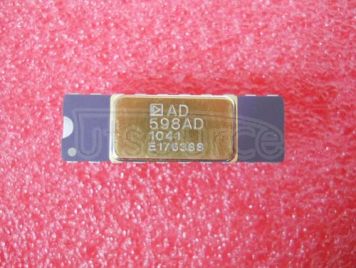
 Required
 signal conditioning subsystem. It is used in conjunction with LVDTs to convert transducer mechanical position to a unipolar or bipolar dc voltage with a high degree of accuracy and repeatability. All circuit functions are included on the chip. With the addition of a few external passive components to set frequency and gain, the AD598 converts the raw LVDT secondary output to a scaled dc signal. The device can also be used with RVDT transducers.
The AD598 contains a low distortion sine wave oscillator to drive the LVDT primary. The LVDT secondary output consists of two sine waves that drive the AD598 directly. The AD598 operates upon the two signals, dividing their difference by their sum, producing a scaled unipolar or bipolar dc output.
The AD598 uses a unique ratiometric architecture (patent pending) to eliminate several of the disadvantages associated with traditional approaches to LVDT interfacing. The benefits of this new circuit are: no adjustments are necessary, transformer null voltage and primary to secondary phase shift does not affect system accuracy, temperature stability is improved, and transducer interchangeability is improved.")