FEATURES Single Chip Solution, Contains Internal Oscillator and
Voltage Reference No Adjustments Required Insensitive to Transducer Null Voltage Insensitive to Primary to Secondary Phase Shifts DC Output Proportional to Position to 20 kHz Frequency Range Single or Dual Supply Operation Unipolar or Bipolar Output Will Operate a Remote LVDT to 300 Feet Position Output Can Drive to 1000 Feet of Cable Will Also Interface to an RVDT Outstanding Performance
Linearity: of FS max Output Voltage: 11 V min Gain Drift: 50 ppm/C of FS max Offset Drift: 50 ppm/C of FS max
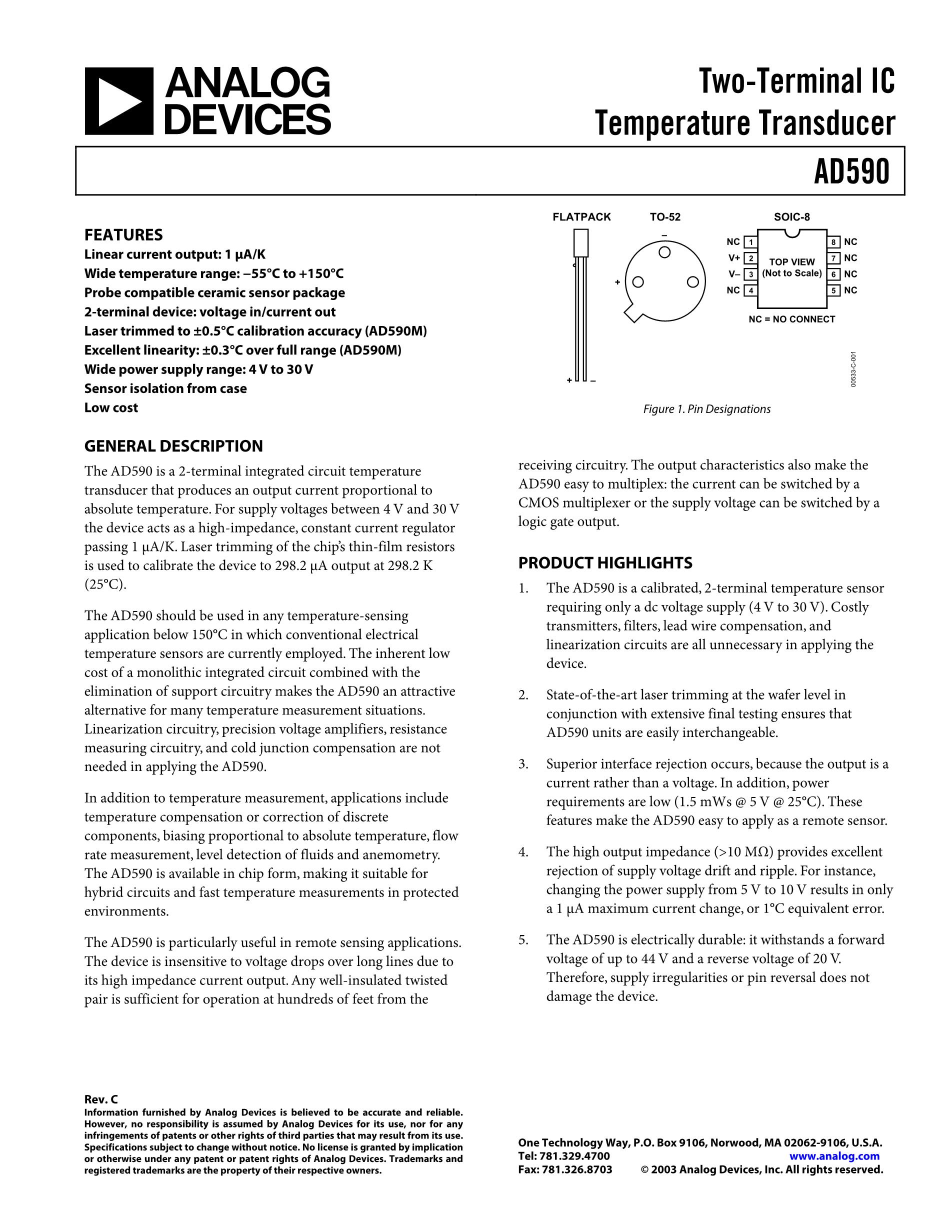
PRODUCT DESCRIPTION The is a complete, monolithic Linear Variable Differential Transformer (LVDT) signal conditioning subsystem. It is used in conjunction with LVDTs to convert transducer mechanical position to a unipolar or bipolar dc voltage with a high degree of accuracy and repeatability. All circuit functions are included on the chip. With the addition of a few external passive components to set frequency and gain, the AD598 converts the raw LVDT secondary output to a scaled dc signal. The device can also be used with RVDT transducers.
The AD598 contains a low distortion sine wave oscillator to drive the LVDT primary. The LVDT secondary output consists of two sine waves that drive the AD598 directly. The AD598 operates upon the two signals, dividing their difference by their sum, producing a scaled unipolar or bipolar dc output.
The AD598 uses a unique ratiometric architecture (patent pending) to eliminate several of the disadvantages associated with traditional approaches to LVDT interfacing. The benefits of this new circuit are: no adjustments are necessary, transformer null voltage and primary to secondary phase shift does not affect system accuracy, temperature stability is improved, and transducer interchangeability is improved.
PRODUCT HIGHLIGHTS 1. The AD598 offers a monolithic solution to LVDT and
RVDT signal conditioning problems; few extra passive components are required to complete the conversion from mechanical position to dc voltage and no adjustments are required.
2. The AD598 can be used with many different types of LVDTs because the circuit accommodates a wide range of input and output voltages and frequencies; the AD598 can drive an LVDT primary with 24 V rms and accept secondary input levels as low 100 mV rms.
3. The to 20 kHz LVDT excitation frequency is determined by a single external capacitor. The AD598 input signal need not be synchronous with the LVDT primary drive. This means that an external primary excitation, such as the 400 Hz power mains in aircraft, can be used.
4. The AD598 uses a ratiometric decoding scheme such that primary to secondary phase shifts and transducer null voltage have absolutely no effect on overall circuit performance.
5. Multiple LVDTs can be driven by a single AD598, either in series or parallel as long as power dissipation limits are not exceeded. The excitation output is thermally protected.
6. The AD598 may be used in telemetry applications or in hostile environments where the interface electronics may be remote from the LVDT. The AD598 can drive an LVDT at the end of 300 feet of cable, since the circuit is not affected by phase shifts or absolute signal magnitudes. The position output can drive as much as 1000 feet of cable.
7. The AD598 may be used as a loop integrator in the design of simple electromechanical servo loops.
Information furnished by Analog Devices is believed to be accurate and reliable. However, no responsibility is assumed by Analog Devices for its use, nor for any infringements of patents or other rights of third parties which may result from its use. No license is granted by implication or otherwise under any patent or patent rights of Analog Devices.
Output Voltage Range (TMIN to TMAX) Output Current (TMIN to TMAX) Short Circuit Current Nonlinearity3 (TMIN to TMAX) Gain Error4
Offset Drift Excitation Voltage Rejection6 Power Supply Rejection 18 V)
PSRR Gain (TMIN to TMAX) PSRR Offset (TMIN to TMAX) Common-Mode Rejection 3 V) CMRR Gain (TMIN to TMAX) CMRR Offset (TMIN to TMAX) Output Ripple7
SIGNAL INPUT CHARACTERISTICS Signal Voltage Input Impedance Input Bias Current (AIN and BIN) Signal Reference Bias Current Excitation Frequency
POWER SUPPLY REQUIREMENTS Operating Range Dual Supply Operation 10 V Output) Single Supply Operation +10 V Output 10 V Output Current (No Load at Signal and Excitation Outputs) TMIN to TMAX
NOTES 1VA and VB represent the Mean Average Deviation (MAD) of the detected sine waves. Note that for this Transfer Function to linearly represent positive displacement, the sum of VA and VB of the LVDT must remain constant with stroke length. See "Theory of Operation." Also see Figures 7 and 12 for R2. 2From TMIN, to TMAX, the overall error due to the AD598 alone is determined by combining gain error, gain drift and offset drift. For example the worst case overall error for the AD598AD from TMIN to TMAX is calculated as follows: overall error = gain error +25°C 1% full scale) + gain drift from +25°C (50 ppm/°C +65°C) + offset drift from +25°C (50 ppm/°C 1.65% of full scale. Note that 1000 ppm of full scale equals 0.1% of full scale. Full scale is defined as the voltage difference between the maximum positive and maximum negative output. 3Nonlinearity of the AD598 only, in units of ppm of full scale. Nonlinearity is defined as the maximum measured deviation of the AD598 output voltage from a
straight line. The straight line is determined by connecting the maximum produced full-scale negative voltage with the maximum produced full-scale positive voltage. 4See Transfer Function. 5This offset refers to the (VAVB)/(VA+VB) input spanning a full-scale range ± 1. [For (VAVB)/(VA+VB) to equal +1, VB must equal zero volts; and correspondingly for (VAVB)/(VA+VB) to equal 1, VA must equal zero volts. Note that offset errors do not allow accurate use of zero magnitude inputs, practical inputs are limited 100 mV rms.] The ± 1 span is a convenient reference point to define offset referred to input. For example, with this input span a value 20 k would give VOUT span a value ± 10 volts. Caution, most LVDTs will typically exercise less of the ((V AVB))/((VA+VB)) input span and thus require a larger value R2 to produce the 10 V output span. In this case the offset is correspondingly magnified when referred to the output voltage. For example, a Schaevitz E100 LVDT
requires 80.2 k for R2 to produce 10.69 V output and (VAVB)/(VA+VB) equals 0.27. This ratio may be determined from the graph shown in Figure 18, (VAVB)/(VA+VB) (1.71 V rms rms)/(1.71 V rms 0.99 V rms). The maximum offset value referred to the 10.69 V output may be determined by multiplying the maximum value shown in the data sheet by 1/0.27 which equals ± 3.7% maximum. Similarly, to determine the maximum values of offset drift, offset CMRR and offset PSRR when referred to the 10.69 V output, these data sheet values should also be multiplied by (1/0.27). For this example for the AD598AD the maximum values of offset drift, PSRR offset and CMRR offset would be: 185 ppm/ °C of FS; 741 ppm/V and 741 ppm/V respectively when referred to the 10.69 V output. 6For example, if the excitation to the primary changes by 1 dB, the gain of the system will change by typically 100 ppm. 7Output ripple is a function of the AD598 bandwidth determined C2, C3 and C4. See Figures 16 and 8R1 is shown in Figures 7 and 12. 9Excitation voltage drift is not an important specification because of the ratiometric operation of the AD598.
Specifications shown in boldface are tested on all production units at final electrical test. Results from those tested are used to calculate outgoing quality levels. All
min and max specifications are guaranteed, although only those shown in boldface are tested on all production units.
Total Supply Voltage +VS to VS. +36 V Storage Temperature Range
to +85°C Lead Temperature Range (Soldering 60 sec). +300°C Power Dissipation 1.2 W Derates Above +65°C. 12 mW/°C
17 SIGNAL REFERENCE 16 SIGNAL OUTPUT 15 FEEDBACK 14 OUTPUT FILTER


 Required
 signal conditioning subsystem. It is used in conjunction with LVDTs to convert transducer mechanical position to a unipolar or bipolar dc voltage with a high degree of accuracy and repeatability. All circuit functions are included on the chip. With the addition of a few external passive components to set frequency and gain, the AD598 converts the raw LVDT secondary output to a scaled dc signal. The device can also be used with RVDT transducers.
The AD598 contains a low distortion sine wave oscillator to drive the LVDT primary. The LVDT secondary output consists of two sine waves that drive the AD598 directly. The AD598 operates upon the two signals, dividing their difference by their sum, producing a scaled unipolar or bipolar dc output.
The AD598 uses a unique ratiometric architecture (patent pending) to eliminate several of the disadvantages associated with traditional approaches to LVDT interfacing. The benefits of this new circuit are: no adjustments are necessary, transformer null voltage and primary to secondary phase shift does not affect system accuracy, temperature stability is improved, and transducer interchangeability is improved.")