


 Required
≥1:
US $0.72644

Buy(0)
Inquiry(0)

Dear customers, due to the implementation of the GDPR policy in Europe, UTSOURCE has also made adjustment accordingly to meet the policy requirements. Please read the new privacy policy carefully and this window will no longer pop up after you accept it.
Delivery Address
+ Add Address
The new shipping address
* Please fill in the cell phone number correctly to make sure that you can receive the tracking info in time.
Country CodeSearch results filter:
 Utsource
Description: The CD4013BCN is a dual D-type flip-flop with complementary outputs. It has two independent data inputs (D and D) and two independent clock inputs (CP and CP). Features: * High speed: tp
Stock:10000
Minimum:4
Favorite
Description: The MC74ACT377N is a 3-state octal D-type flip-flop with a common Clock (CP) and Output Enable (OE) inputs. Features: Wide Operating Voltage Range of 2.0 V to 6.0 V High Speed Oper
Stock:10000
Minimum:5
Favorite
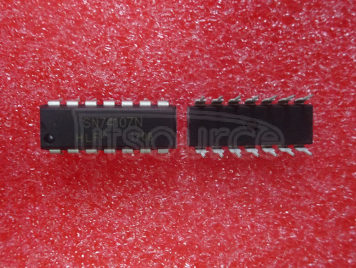
SN74107N is a high-level logic device that is part of the 74xx series of integrated circuits. It is a 14-pin DIP (dual in-line package) that contains four independent two-input NAND gates. Descriptio
Stock:99999
Minimum:100
Favorite
Stock:10000
Minimum:1
Favorite
Manufacturer: NXP Description: The 74HC174D,653 is a high-speed Si-gate CMOS device and is pin compatible with low-power Schottky TTL (LSTTL). It is specified in compliance with JEDEC standard no. 7A.
Stock:10000
Minimum:100
Favorite
Description: The MC74ACT74N is a dual D-type flip-flop with individual data, set, reset, and clock inputs and Q and Q outputs. Features: Low Power Consumption High Speed Operation Outputs S
Stock:10000
Minimum:4
Favorite
Description: The CD74HCT534E is a high-speed CMOS 8-bit buffer/line driver fabricated with silicon gate C2MOS technology. Features: - High-speed operation: tPD = 8.0 ns (typical) at VCC = 5 V - Low p
Stock:10000
Minimum:2
Favorite
Description: The MC74HC174A is an 8-bit D-type flip-flop with a common clock and asynchronous reset. Features: - High speed: tpd = 7.5 ns (typical) at VCC = 5 V - Low power dissipation: ICC = 4 μA (m
Stock:10000
Minimum:14
Favorite
Stock:99799
Minimum:200
Favorite
Manufacturer: NXP Description: Dual D-Type Flip-Flop Features: Low power consumption High noise immunity Low input current High speed operation Outputs source/sink 24 mA Outputs compatib
Stock:10000
Minimum:10
Favorite
Description: The MM74HC74AM is a dual D-type flip-flop with set and reset inputs. Features: Inputs Include Clamp Diodes Outputs Source/Sink 24 mA Latch-Up Performance Exceeds 250 mA Per JESD 78, Cl
Stock:10000
Minimum:12
Favorite
Description: Dual JK Flip-Flop Features: - Low power Schottky TTL (LSTTL) - Inputs compatible with standard TTL outputs - Outputs source/sink 24 mA - Typical propagation delay: 8 ns - Typical p
Stock:10000
Minimum:1
Favorite
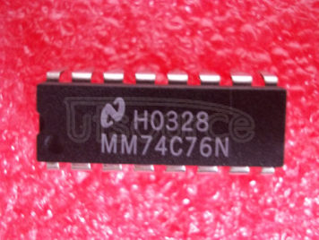
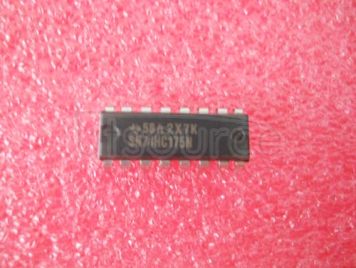
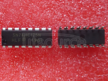
SN74HC175N is a Quad D-type flip-flop IC with a DIP-16 package manufactured by Texas Instruments. It is a high-speed CMOS logic device that is designed for low-power operation. Description: The SN74H
Stock:10000
Minimum:2
Favorite
Description: The CD40174BCN is a 4-bit static shift register with parallel inputs and serial outputs. Features: 4-bit static shift register Parallel inputs and serial outputs Low power consumptio
Stock:10000
Minimum:2
Favorite
Stock:99999
Minimum:200
Favorite
Description: The SN74ACT74DE4 is a Dual D-Type Flip-Flop with Preset and Clear from Texas Instruments. Features: * Low power consumption * High speed * Low noise * High output drive capability * Inpu
Stock:10000
Minimum:5
Favorite
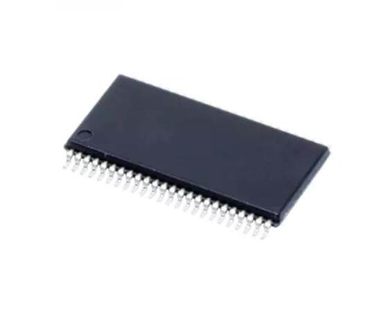
TSSOP-48
TI Texas Instruments
1719+
8-Bit D-Type Flip-Flop
Stock:10000
Minimum:5
Favorite
Stock:99499
Minimum:500
Favorite
Description: The 74LVTH16374MTDX is a 16-bit dual-supply bus transceiver with 3-state outputs. It is designed for asynchronous two-way communication between data buses. Features: Low voltage operati
Stock:10000
Minimum:10
Favorite
Description: The 74ACT175SCX is a high-speed 4-bit register with 3-state outputs. It is designed for use in high-performance memory and bus-oriented systems. Features: High-speed performance: tpd =
Stock:10000
Minimum:14
Favorite

Stop production experts, we can provide a large number of electronic components that have been stopped production and are difficult to find, to facilitate the maintenance company
Stock
Toll-Free Call
(888) 766 5577 USA & Canada
+52 5515436027
+52 5515436028 Mexico
+49 6931090199 Germany
+55 21 3609 8727 Brazil
(800) 137235 Italy
(900) 649657 Spain
+1 (312) 899-4831 USA
+49 15217848563 Germany
+52 55 7637 4368 Mexico
GLOBAL PAYMENTS
Global logistics