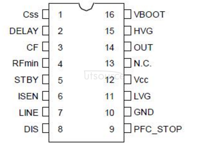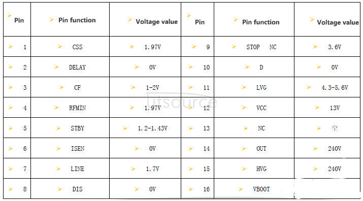

L6599D pin function
1. Css: soft start end. This pin is connected to ground (GND) with a capacitor Css, and pin 4 (RFmin) is connected with a resistor Rss to determine the highest operating frequency during soft-start. When Vcc (pin 12) "UVLO (low voltage lockout), LINE (pin 7) "1.25V or "6V, DIS (pin 8)" 1.85V (forbidden terminal), ISEN (pin 6) "1.5V, DELAY ( 2 feet) "3.5V, and when the voltage of ISEN exceeds 0.8V or exceeds 0.75V for a long time, the chip is turned off, and the capacitor Css is discharged through the internal switch of the chip to make the restart process a soft start.
2. DELAY: Overload current delay shutdown terminal. This end is connected to the ground in parallel with a resistor Rd and a capacitor Cd each to set the longest duration of the overload current. When the voltage of the ISEN pin exceeds 0.8V, the chip will charge Cd through a constant current source of 150uA. When the charging voltage exceeds 2.0V, the output of the chip will be turned off and the soft-start capacitor Css will be discharged. After the circuit is turned off, the overcurrent signal disappears, the 3.5V power supply for charging Cd inside the chip is turned off, and the electricity on Cd is discharged through Rd. When the voltage is lower than 0.3V, the soft start starts. In this way, in the overload or short circuit state, the chip works in an intermittent working state over and over again. (Rd should not be less than 2V/150uA=13.3kΩ. The larger the Rd, the shorter the allowable over-current time and the longer the turn-off time.)
3. CF: Timing capacitor. Connect a capacitor Cf to the ground, and the 4-pin RFmin to the ground to match the switching frequency of the programmable oscillator.
4. RFmin: Minimum oscillation frequency setting. Pin 4 provides 2V reference voltage, and connect a resistor RFmin from pin 4 to ground to set the lowest oscillation frequency. Connect a resistor RFmax from pin 4 and ground through the optocoupler controlled by the feedback loop, which will be used to adjust the oscillation frequency of the switch. RFmax is the highest operating frequency setting resistance. The RC network between pin 4-pin 1-GND realizes soft start.
5. STBY: Standby, the threshold of intermittent working mode (<1.25V). Pin 5 is controlled by the feedback voltage and compared with the internal 1.25V reference voltage. If the voltage of pin 5 is lower than the reference voltage of 1.25V, the chip is in a static state, and there is only a small static operating current. When the voltage of pin 5 exceeds the reference voltage of 50mV, the chip restarts to work. During this process, the soft start does not work. When the load drops below a certain level (light load), through RFmax and optocoupler (see the structure diagram), this function enables the chip to implement intermittent working mode. If there is no circuit connection between pin 5 and pin 4, the intermittent operation mode is not enabled.
6. ISEN: Current detection signal input terminal. Pin 6 detects the current in the main loop through a resistance shunt or a capacitive current sensor. This input is not intended to achieve cycle-by-cycle control, so the average current information must be obtained through filtering. When the voltage exceeds the 0.8V threshold (there is a 50mV hysteresis, that is, once it crosses 0.8V, then as long as it does not fall below 0.75V, it still works), the soft-start capacitor on pin 1 is discharged internally by the chip, and the operating frequency is increased to limit Power output. In the case of a short circuit in the main circuit, this usually makes the peak current of the circuit almost constant. Taking into account that the overcurrent time is set by pin 2, if the current continues to increase, despite the increase in frequency, when the voltage exceeds the reference voltage (1.5V) of another comparator, the driver will shut down and the energy loss will almost return to the level before the start. The detection information is blocked, and the chip will be restarted only when the power supply voltage Vcc is lower than UVLO. If this function is not used, please ground pin 4.
7. LINE: Input voltage detection. This end is protected by a voltage divider resistor sampling AC or DC input voltage (between the system and the PFC). When the detection voltage is lower than 1.25V, the output is turned off (non-latching) and the soft start capacitor is released. Restart soft-start when the voltage is higher than 1.25V. This comparator has hysteresis: if the detection voltage is lower than 1.25V, the internal 15uA constant current source is turned on. Connect a capacitor to pin 7 to ground to eliminate noise interference. The pin voltage is limited by the internal 6.3V Zener diode. The conduction of the 6.3V Zener diode makes the output of the chip turn off (non-latching). If this function is not used, the voltage of this pin is between 1.25V and 6V.
8.DIS: Disable, the latching drive is closed. This pin is connected to a comparator internally. When the voltage of this pin exceeds 1.85V, the chip will shut down in a latched manner. Only when the chip's operating voltage Vcc is lowered below the UVLO threshold can it restart. If you do not use this function, please ground this pin.
9. PFC_STOP: Open the control channel of the PFC (power factor correction) controller. The opening of this pin is to stop the work of the PFC controller to achieve protection purposes or intermittent working mode. When the chip is turned off by DIS"1.85V, ISEN"1.5V, LINE"6V and STBY"1.25V, the 9-pin output is pulled low. When the DELAY terminal voltage exceeds 2V and does not return to below 0.3V, this terminal is also pulled down. During UVLO (low voltage lockout), this pin is open. Allow this foot to be left unused.
10. GND: chip ground. The loop current is the sum of the low-side gate drive current and the chip bias operating current. All relevant grounds should be connected to this pin and separated from the pulse control loop.
11.LVG: Low-end gate drive output. This pin can provide a small drive current of 0.3A. Source 0.8A (?). Sink (?) The peak current drives the low-end MOS tube of the half-bridge circuit. During UVLO, LVG is pulled down to ground.
12.Vcc: The power supply includes the signal part of the chip and the gate drive of the low-end MOS tube. Connecting a small filter capacitor (0.1uF) helps the chip signal circuit to obtain a clean bias voltage.
13.N.C.: Empty pin, used for high voltage isolation, to increase the distance between Vcc and pin 14. There is no connection inside the pin, which is isolated from high voltage, and makes it possible to meet the requirements of safety regulations (leakage distance) on the PCB.
14.OUT: Floating ground driven by high-side gate. Provide a current return loop for the high-side gate drive current. The layout should be careful to avoid too large burrs below ground.
15. HVG: High-end floating gate drive output. This pin can provide a small drive current of 0.3A. Source 0.8A (?). Sink (?) the peak current to drive the upper MOS transistor of the half-bridge circuit. There is a resistor connected to pin 14 (OUT) through the chip to ensure that it is not driven floating during UVLO.
16.VBOOT: High-end gate drive floating power supply. A bootstrap capacitor Cboot is connected between pin 16 (Vboot) and pin 14 (OUT), which is driven synchronously by a bootstrap diode inside the chip and the low-side gate driver. This patented structure replaces the commonly used external diode.
Comments


participate in discussions
Please login ? to participate in the comments
New customer Start here.