


 Required
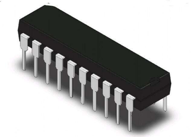
≥1:
US $1.22936

Buy(0)
Inquiry(0)

Dear customers, due to the implementation of the GDPR policy in Europe, UTSOURCE has also made adjustment accordingly to meet the policy requirements. Please read the new privacy policy carefully and this window will no longer pop up after you accept it.
Delivery Address
+ Add Address
The new shipping address
* Please fill in the cell phone number correctly to make sure that you can receive the tracking info in time.
Country CodeSearch results filter:
 Utsource
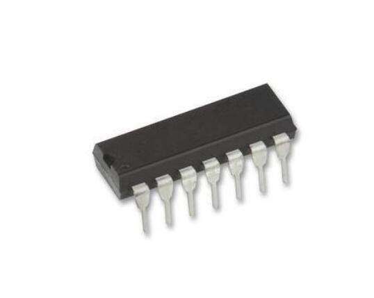
DIP20
Ns/fsc
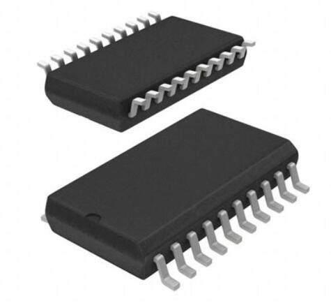
These monolithic, positive-edge-triggered flip-flops utilize TTL circuitry to implement D-type flip-flop logic with an enable input. The 'LS377, 'LS378, and 'LS379 devices are similar to 'LS273, 'LS174, and 'LS175, respectively, but feature a common enable instead of a common clear. Information at the D inputs meeting the setup time requirements is transferred to the Q outputs on the positive-going edge of the clock pulse if the enable input G\ is low. Clock triggering occurs at a particular voltage level and is not directly related to the transition time of the positive-going pulse. When the clock input is at either the high or low level, the D input signal has no effect at the output. The circuits are designed to prevent false clocking by transitions at the G\ input. These flip-flops are guaranteed to respond to clock frequencies ranging from 0 to 30 MHz while maximum clock frequency is typically 40 megahertz. Typical power dissipation is 10 milliwatts per flip-flop.
Stock:10000
Minimum:2
Favorite
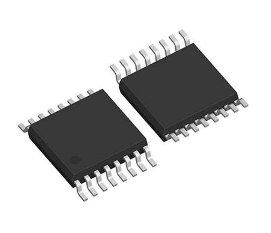
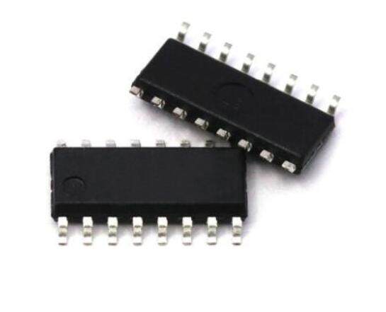
SOP-20
TI9
These monolithic, positive-edge-triggered flip-flops utilize TTL circuitry to implement D-type flip-flop logic with an enable input. The 'LS377, 'LS378, and 'LS379 devices are similar to 'LS273, 'LS174, and 'LS175, respectively, but feature a common enable instead of a common clear. Information at the D inputs meeting the setup time requirements is transferred to the Q outputs on the positive-going edge of the clock pulse if the enable input G\ is low. Clock triggering occurs at a particular voltage level and is not directly related to the transition time of the positive-going pulse. When the clock input is at either the high or low level, the D input signal has no effect at the output. The circuits are designed to prevent false clocking by transitions at the G\ input. These flip-flops are guaranteed to respond to clock frequencies ranging from 0 to 30 MHz while maximum clock frequency is typically 40 megahertz. Typical power dissipation is 10 milliwatts per flip-flop.
Stock:10000
Minimum:3
Favorite
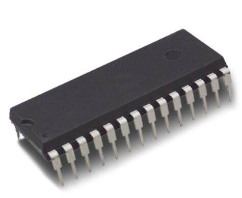
DIP24
Texas Instruments
00+
ti SN74ALS577A, Octal D-type Edge-triggered Flip-flops With 3-State Outputs
Description: The SN74ALS577ANT is a high-speed, low-power, octal D-type flip-flop with 3-state outputs. Features: * Low power consumption * High-speed operation * 3-state outputs * TTL-compatible inp
Stock:10000
Minimum:2
Favorite
SOP-20
FSC
Octal D Flip-Flop with Clear; Package: SOIC-Wide; No of Pins: 20; Container: Rail
Stock:10000
Minimum:6
Favorite
DIP20
TI Texas Instruments
1547+
These monolithic, positive-edge-triggered flip-flops utilize TTL circuitry to implement D-type flip-flop logic with an enable input. The 'LS377, 'LS378, and 'LS379 devices are similar to 'LS273, 'LS174, and 'LS175, respectively, but feature a common enable instead of a common clear. Information at the D inputs meeting the setup time requirements is transferred to the Q outputs on the positive-going edge of the clock pulse if the enable input G\ is low. Clock triggering occurs at a particular voltage level and is not directly related to the transition time of the positive-going pulse. When the clock input is at either the high or low level, the D input signal has no effect at the output. The circuits are designed to prevent false clocking by transitions at the G\ input. These flip-flops are guaranteed to respond to clock frequencies ranging from 0 to 30 MHz while maximum clock frequency is typically 40 megahertz. Typical power dissipation is 10 milliwatts per flip-flop.
Description: The CD74FCT374E is a high-speed CMOS Octal D-type Flip-Flop with 3-state outputs fabricated with silicon gate CMOS technology. Features: High Speed Operation: tPD = 10ns (typ) at VCC =
Stock:10000
Minimum:2
Favorite
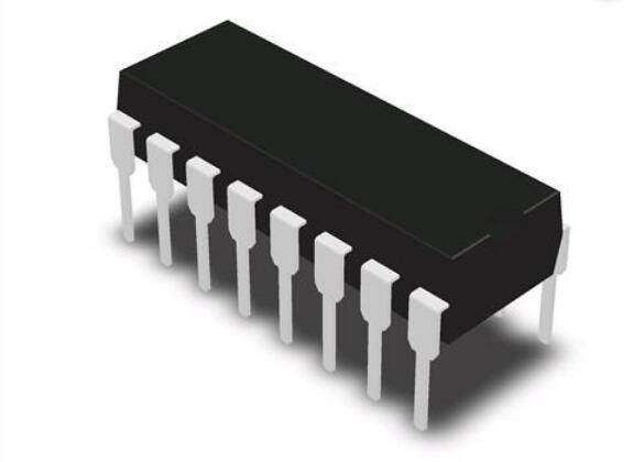
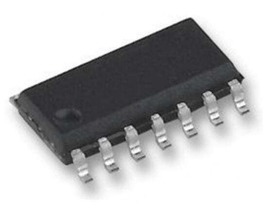
DIP-16
MIT
82
These monolithic, positive-edge-triggered flip-flops utilize TTL circuitry to implement D-type flip-flop logic with an enable input. The 'LS377, 'LS378, and 'LS379 devices are similar to 'LS273, 'LS174, and 'LS175, respectively, but feature a common enable instead of a common clear. Information at the D inputs meeting the setup time requirements is transferred to the Q outputs on the positive-going edge of the clock pulse if the enable input G\ is low. Clock triggering occurs at a particular voltage level and is not directly related to the transition time of the positive-going pulse. When the clock input is at either the high or low level, the D input signal has no effect at the output. The circuits are designed to prevent false clocking by transitions at the G\ input. These flip-flops are guaranteed to respond to clock frequencies ranging from 0 to 30 MHz while maximum clock frequency is typically 40 megahertz. Typical power dissipation is 10 milliwatts per flip-flop.
Description: Dual Monostable Multivibrator Features: High Voltage Type (20V Rating) Outputs Source/Sink 24mA Retriggerable Output Pulse Width Control by Two External Resistors and Capacitor Input
Stock:10000
Minimum:4
Favorite
SOP20
1140+
These monolithic, positive-edge-triggered flip-flops utilize TTL circuitry to implement D-type flip-flop logic with an enable input. The 'LS377, 'LS378, and 'LS379 devices are similar to 'LS273, 'LS174, and 'LS175, respectively, but feature a common enable instead of a common clear. Information at the D inputs meeting the setup time requirements is transferred to the Q outputs on the positive-going edge of the clock pulse if the enable input G\ is low. Clock triggering occurs at a particular voltage level and is not directly related to the transition time of the positive-going pulse. When the clock input is at either the high or low level, the D input signal has no effect at the output. The circuits are designed to prevent false clocking by transitions at the G\ input. These flip-flops are guaranteed to respond to clock frequencies ranging from 0 to 30 MHz while maximum clock frequency is typically 40 megahertz. Typical power dissipation is 10 milliwatts per flip-flop.
Stock:10000
Minimum:4
Favorite
DIP-16
FSC
0516+
16-Bit Buffer/Line Driver with 3-STATE Outputs; Package: SSOP; No of Pins: 48; Container: Tape & Reel
Stock:10000
Minimum:3
Favorite
Description: Quad D-Type Flip-Flop Features: Low Power Consumption Low Input Current High Noise Immunity High Speed Performance Outputs Source/Sink 24 mA Inputs Accept Voltages to 5
Stock:10000
Minimum:4
Favorite
SOP14
Ns/fsc
00+
These monolithic, positive-edge-triggered flip-flops utilize TTL circuitry to implement D-type flip-flop logic with an enable input. The 'LS377, 'LS378, and 'LS379 devices are similar to 'LS273, 'LS174, and 'LS175, respectively, but feature a common enable instead of a common clear. Information at the D inputs meeting the setup time requirements is transferred to the Q outputs on the positive-going edge of the clock pulse if the enable input G\ is low. Clock triggering occurs at a particular voltage level and is not directly related to the transition time of the positive-going pulse. When the clock input is at either the high or low level, the D input signal has no effect at the output. The circuits are designed to prevent false clocking by transitions at the G\ input. These flip-flops are guaranteed to respond to clock frequencies ranging from 0 to 30 MHz while maximum clock frequency is typically 40 megahertz. Typical power dissipation is 10 milliwatts per flip-flop.
Stock:10000
Minimum:13
Favorite
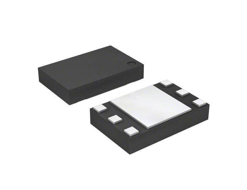
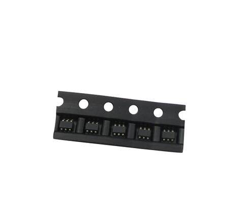
SOT-363/MAA06A
Fairchild
05+
These monolithic, positive-edge-triggered flip-flops utilize TTL circuitry to implement D-type flip-flop logic with an enable input. The 'LS377, 'LS378, and 'LS379 devices are similar to 'LS273, 'LS174, and 'LS175, respectively, but feature a common enable instead of a common clear. Information at the D inputs meeting the setup time requirements is transferred to the Q outputs on the positive-going edge of the clock pulse if the enable input G\ is low. Clock triggering occurs at a particular voltage level and is not directly related to the transition time of the positive-going pulse. When the clock input is at either the high or low level, the D input signal has no effect at the output. The circuits are designed to prevent false clocking by transitions at the G\ input. These flip-flops are guaranteed to respond to clock frequencies ranging from 0 to 30 MHz while maximum clock frequency is typically 40 megahertz. Typical power dissipation is 10 milliwatts per flip-flop.
Description: NC7SZ175P6X is a single inverter gate from Fairchild Semiconductor. It is a low-power, low-voltage, single-gate CMOS device. Features: - Low power consumption - Low voltage operation - H
Stock:10000
Minimum:13
Favorite
SOT-363/MAA06A
Fairchild
05
These monolithic, positive-edge-triggered flip-flops utilize TTL circuitry to implement D-type flip-flop logic with an enable input. The 'LS377, 'LS378, and 'LS379 devices are similar to 'LS273, 'LS174, and 'LS175, respectively, but feature a common enable instead of a common clear. Information at the D inputs meeting the setup time requirements is transferred to the Q outputs on the positive-going edge of the clock pulse if the enable input G\ is low. Clock triggering occurs at a particular voltage level and is not directly related to the transition time of the positive-going pulse. When the clock input is at either the high or low level, the D input signal has no effect at the output. The circuits are designed to prevent false clocking by transitions at the G\ input. These flip-flops are guaranteed to respond to clock frequencies ranging from 0 to 30 MHz while maximum clock frequency is typically 40 megahertz. Typical power dissipation is 10 milliwatts per flip-flop.
Description: NC7SZ175P6X is a single inverter gate from Fairchild Semiconductor. It is a low-power, low-voltage, single-gate CMOS device. Features: - Low power consumption - Low voltage operation - H
Stock:10000
Minimum:13
Favorite
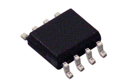
SOP8
STMicroelectronics
07+
These monolithic, positive-edge-triggered flip-flops utilize TTL circuitry to implement D-type flip-flop logic with an enable input. The 'LS377, 'LS378, and 'LS379 devices are similar to 'LS273, 'LS174, and 'LS175, respectively, but feature a common enable instead of a common clear. Information at the D inputs meeting the setup time requirements is transferred to the Q outputs on the positive-going edge of the clock pulse if the enable input G\ is low. Clock triggering occurs at a particular voltage level and is not directly related to the transition time of the positive-going pulse. When the clock input is at either the high or low level, the D input signal has no effect at the output. The circuits are designed to prevent false clocking by transitions at the G\ input. These flip-flops are guaranteed to respond to clock frequencies ranging from 0 to 30 MHz while maximum clock frequency is typically 40 megahertz. Typical power dissipation is 10 milliwatts per flip-flop.
Description: Quad 2-Input NAND Schmitt Trigger Features: - Low power Schottky technology - High noise immunity - High input impedance - Low input current - Outputs source/sink up to 20 mA - TTL compa
Stock:10000
Minimum:4
Favorite
Description: Dual D-Type Flip-Flop Features: - High-speed performance - Low power consumption - Inputs and outputs are TTL compatible - Outputs can be wired ORed Applications: - Frequency dividers -
Stock:10000
Minimum:5
Favorite
DIP-14
National Semiconductor
Dual D Positive-Edge-Triggered Flip-Flops with Preset and Clear; Package: DIP; No of Pins: 14; Container: Rail
Stock:10000
Minimum:2
Favorite
Description: Hex D-Type Flip-Flop Features: High-Voltage Types (20V Rating) Input Clamp Diodes Limit High-Level Input Voltage to VCC + 0.5V Outputs Source/Sink 24 mA Output Clamp Diodes Limi
Stock:10000
Minimum:2
Favorite
SOP
FSC
02+
These monolithic, positive-edge-triggered flip-flops utilize TTL circuitry to implement D-type flip-flop logic with an enable input. The 'LS377, 'LS378, and 'LS379 devices are similar to 'LS273, 'LS174, and 'LS175, respectively, but feature a common enable instead of a common clear. Information at the D inputs meeting the setup time requirements is transferred to the Q outputs on the positive-going edge of the clock pulse if the enable input G\ is low. Clock triggering occurs at a particular voltage level and is not directly related to the transition time of the positive-going pulse. When the clock input is at either the high or low level, the D input signal has no effect at the output. The circuits are designed to prevent false clocking by transitions at the G\ input. These flip-flops are guaranteed to respond to clock frequencies ranging from 0 to 30 MHz while maximum clock frequency is typically 40 megahertz. Typical power dissipation is 10 milliwatts per flip-flop.
Description: Dual D-Type Flip-Flop Features: High-Voltage Types (20V Rating) Medium Speed Operation Outputs Source/Sink 24mA Schmitt Trigger Inputs Input Clamping Diodes Standardized Symmetrical
Stock:10000
Minimum:3
Favorite
Description: The 74ACT11074N is a high-speed CMOS octal D-type flip-flop with 3-state outputs fabricated with TI's advanced silicon-gate CMOS technology. Features: High-speed performance: tPD = 11.
Stock:10000
Minimum:2
Favorite
The 74C74 is a dual D-type flip-flop with a clock and clear inputs. It is a 14-pin dual in-line package (DIP-14) manufactured by Texas Instruments (TI) and National Semiconductor (NS). Description: T
Stock:10000
Minimum:3
Favorite
DIP20
These monolithic, positive-edge-triggered flip-flops utilize TTL circuitry to implement D-type flip-flop logic with an enable input. The 'LS377, 'LS378, and 'LS379 devices are similar to 'LS273, 'LS174, and 'LS175, respectively, but feature a common enable instead of a common clear. Information at the D inputs meeting the setup time requirements is transferred to the Q outputs on the positive-going edge of the clock pulse if the enable input G\ is low. Clock triggering occurs at a particular voltage level and is not directly related to the transition time of the positive-going pulse. When the clock input is at either the high or low level, the D input signal has no effect at the output. The circuits are designed to prevent false clocking by transitions at the G\ input. These flip-flops are guaranteed to respond to clock frequencies ranging from 0 to 30 MHz while maximum clock frequency is typically 40 megahertz. Typical power dissipation is 10 milliwatts per flip-flop.
Stock:10000
Minimum:2
Favorite

Stop production experts, we can provide a large number of electronic components that have been stopped production and are difficult to find, to facilitate the maintenance company
Stock
Toll-Free Call
(888) 766 5577 USA & Canada
+52 5515436027
+52 5515436028 Mexico
+49 6931090199 Germany
+55 21 3609 8727 Brazil
(800) 137235 Italy
(900) 649657 Spain
+1 (312) 899-4831 USA
+49 15217848563 Germany
+52 55 7637 4368 Mexico
GLOBAL PAYMENTS
Global logistics